Agenda
Microelectronics colloquium
- Thursday, 12 June 2025
- 16:00-17:00
- EEMCS, lecture hall Chip
From Graphene towards Van der Waals Heterostructures: The National Scalable Atomic Processing Line (SAP-NL)
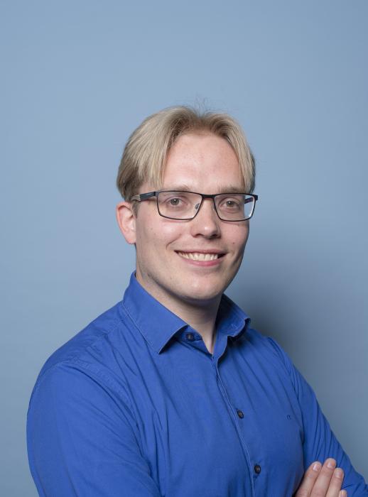
Sten Vollebregt
From Graphene towards Van der Waals Heterostructures: The National Scalable Atomic Processing Line (SAP-NL)
Material innovation has been pivotal for our economy and society and has enabled us to develop faster and more energy-efficient chips, better batteries, solar panels, and communication networks. We are now coming to the point where we can manipulate materials down to the atomic level, which will enable us to create designer materials that are tailored to specific applications. Emerging thin‐film wide bandgap semiconductors and 2D materials are prime candidates for atomically engineered designer materials. At the atomic scale, they exhibit physical phenomena that can be used to deepen our understanding of condensed matter physics and simultaneously be exploited to create novel functional devices, which are potential game changers in broad societal and economic trends such as sustainable energy and smarter digitalization in the internet of everything.
In this talk, I will first provide an overview of the activities on graphene that has been going on within our department for the past decade. This will include applications of graphene as gas sensor, microphone, and the activities with the group of Dr. Giagka on graphene electrodes. Afterwards, I will introduce the to be created national Scalable Atomic Processing line (SAP-NL) that is set to expand our 2D material portfolio and enable the scalable deposition and stacking of 2D materials in Van der Waals heterostructures while keeping their interfaces pristine.
Agenda
- Thu, 12 Jun 2025
- 16:00
- EEMCS, lecture hall Chip
Microelectronics colloquium

Sten Vollebregt
From Graphene towards Van der Waals Heterostructures: The National Scalable Atomic Processing Line (SAP-NL)
Material innovation has been pivotal for our economy and society and has enabled us to develop faster and more energy-efficient chips, better batteries, solar panels, and communication networks.
- Thu, 4 Sep 2025
- 10:00
- Aula Senaatszaal
PhD Thesis Defence

Leiming Du
Sintering Fundamentals of Nano-Metallic Particle Interconnects
- Thu, 4 Sep 2025
- 17:30
- Aula Senaatszaal
PhD Thesis Defence
