Openings at ME
Vacancy not active
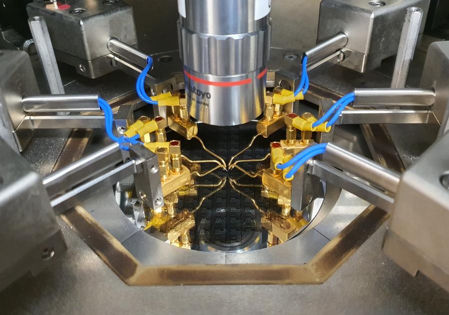
Measurement Lab & Packaging Engineer
Opening for: TechnicianStatus details
| Status: | Closed |
|---|---|
| Announced: | 27 Jul 2020 |
| Closing date: | 15 Aug 2020 |
As a lab engineer you will be supporting students and researchers within the department with their activities related to device packaging and measurements. You will be working in an international team of scientists, and in close collaborations with researchers, as well as MSc and PhD students. Your main responsibilities and activities include:
- Manage and monitor the wafer-scale measurement lab, consisting of semi-automatic probe stations and measurement equipment
- Propose improvements for the lab in terms of innovative products, tools, equipment, software and work methods and support the acquisition
- Support students and researchers in building experimental setups
- Improve and maintain the existing lab infrastructure
- Train students and researcher in usage of the lab infrastructure
- Support students with device packaging related activities like wafer thinning, wafer dicing, (wire) bonding, (flexible) PCB design, etc.
- Support students with system integration related activities like assembly, system-in package assembly, encapsulation, interfacing and testing in a variety of environments (humidity, temperature, etc.)
Requirements
Essential skills:- HBO/BSc/MSc degree or similar in a relevant discipline, such as electrical engineering.
- Experience with electrical device characterisation using equipment such as multimeters, oscilloscopes, semiconductor parameter analysers and network analysers
- Experience with device packaging and system integration
- Willingness to learn new skills on the job, e.g. the use of IC-CAP, longevity testing, etc.
- Demonstrable teamwork and trouble-shooting skills
- Can-do mentality
- Proficiency in written and oral communication in English.
- Strong team mentality and enthusiasm to work in a diverse, international team.
Preference will be given to candidates with the following skills:
- Semiconductor device characterization using software like IC-CAP
- Packaging skills like wire bonding, wafer dicing, etc. Experience with building experiments for electrical, optical and ultrasound device characterisation.
More information