3D System-in-package Design Using Stacked Silicon Submount Technology (3DSiP)
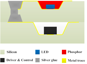
With the increasing demand for miniaturization of portable electronics, higher function integration level and lower cost are major challenges in the semiconductor industry. System-in-Package (SiP) technology is one of the fastest emerging technologies offering highly flexible and low-cost integration and packaging solutions. As the era of intelligence comes, smart electronics have penetrated into many aspects of our daily life, from ambient intelligence to wearable electronics on human bodies. These smart electronic systems consist of not only multiple integrated circuits (ICs) but also passives, sensors, actuators, etc., all of which can be integrated into a single compact package by means of SiP technology. Dramatically worldwide growth of SiP has already been predicted in various applications, including portable electronics, wireless products, sensor systems and smart lighting systems. Substrate plays a significant role in the design of 3D SiP. Silicon makes a well-suited candidate for packaging substrates. Moreover, silicon-based packaging process is inherently compatible with IC/MEMS processes, helping open up new opportunities for 3D heterogeneous integration.

Project data
| Researchers: | Mingzhi Dong, Fabio Santagata, Jia Wei, GuoQi Zhang |
|---|---|
| Starting date: | May 2012 |
| Closing date: | May 2016 |
| Sponsor: | State Key Laboratory of SSL |
| Partners: | Beijing Research Centre |
| Contact: | GuoQi Zhang |