MSc thesis project proposal
Backside contacting of individual signals in multilayer ICs for chip forensics
The term ‘chip forensics’ is used to describe the research of the reverse engineering and modification of (parts of) ICs. This research is found in supply chain verification (did you get what you ordered?), patent infringement investigation (is someone using your IP?) and crime scene investigation (evidence acquisition). The Netherlands Forensic Institute (NFI) focuses on the latter to help, for example, the police with evidence acquisition from smartphones to find the truth in a criminal investigation. In other words, hardware hacking is used to gain access to information.
Modern ICs incorporate multilayer metal interconnect, to facilitate the vast amount of connections to the device layer This ensures the high level of miniaturization for the IC designer, but is a challenging property for chip forensic
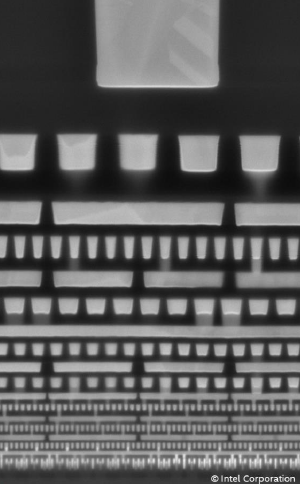
researchers. In the case of a few interconnect layers, the forensic researcher can still observe and access the majority of circuit blocks or signals. However, in technologies with much more interconnect layers (see image), it becomes impossible to interface with specific circuit blocks and/or signals.
In the case of a few interconnect layers, the forensic researcher can still observe and access the majority of circuit blocks or signals. However, in technologies with much more interconnect layers (see image), it becomes impossible to interface with specific circuit blocks and/or signals.
Assignment
The research is performed in both the EKL and NFI labs, depending on the formulated process steps. EKL is located at the Delft University of Technology and NFI is located in Ypenburg. The NFI is a part of the ministry of Justice and Safety and is an independent institute.
The project timeline is 9 months and the starting date is not yet fixed.
The EKL cleanroom facilities are used for wafer level fabrication processes, in an environment with other students and excellent supervision.
The NFI provides access to tools used for chip level modification (such as FIB), expert supervision, and an internship compensation.
Finally, please be informed that a background screening prior to the project start is mandatory for working at NFI
Requirements
The ideal candidate for this project would need the following:
- A strong background in microelectronics
- Good writing and presentation skills
- Takes initiative towards problem solving
- Able to work with fragile samples
- Professional attitude towards IP (not everything can be published)
- Affinity with hardware hacking
If you think you have what it takes to tackle this challenging engineering project, do not hesitate to
contact us for more information.
Contact
dr.ir. Sten Vollebregt
Electronic Components, Technology and Materials Group
Department of Microelectronics
Last modified: 2023-12-05