dr. J.F. Creemer
Electronic Components, Technology and Materials (ECTM), Department of Microelectronics
PhD thesis (Jan 2002): The effect of mechanical stress on bipolar transistor characteristics
Promotor: Paddy French, S. Middelhoek
Expertise: MEMS design and technology
Biography
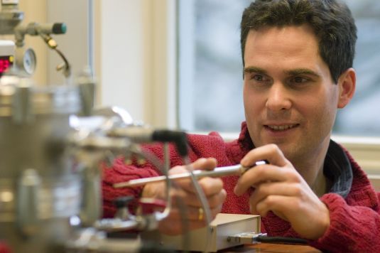
Fredrik Creemer was born in Amsterdam in 1972. He received the M.Sc. degree in electrical engineering in 1995 from Delft University of Technology, Delft, the Netherlands. In 1996 he obtained the DEA degree in electronics from the Universit� Paris-Sud, Orsay, France. He worked towards his PhD degree in the Electronics Instrumentation Laboratory in Delft, which he received in 2002. As a circuit designer he worked with SystematIC Design BV, and as a MEMS designer with the Kavli Institute of Nanoscience in Delft. Currently, he is an Assistant Professor with DIMES (Delft Institute of Microsystems and Nanoelectronics) at Delft University of Technology.
Dr. Creemer�s research interests include MEMS design and technology; in particular, microreactors, nanoparticle characterization, microheaters, MEMS for harsh environments, vacuum devices, thin-film silicon carbide, and wafer-level packaging. With his group he develops a.o. nanoreactors that are used for for in situ microscopy of nanomaterials under industrially relevant conditions. He is author of 22 papers in research journals, 45 papers at peer-reviewed conferences, and he is holding two patents.
Fredrik Creemer is lecturing 'Materials for Nanoelectronics and MEMS' in the MSc programme on Microelectronics. He is co-author and tutor of the design project �EPO-1� for first-year students in Electrical Engineering. He is member of the IEEE and served in the Technical Program Committee of the IEEE Sensors Conference. He was the recipient of the Else Kooi Award in 2002 and the Veni Grant in 2006. In his spare time he likes hiking and swimming. He is council member of the Oecumenical Church of Delft and of MoTiv.
Projects history
MEMS nanoreactors for atomic-scale microscopy of nanomaterials under industrially relevant conditions
MEMS nanoreactors are used to study chemical reactions in high-resolution microscopes
Thin-film encapsulation of MEMS microcavities
With zero-level packaging or thin-film encapsulation, MEMS are already sealed during wafer processing.
- All-SiC surface micromachined nanoreactor for in-situ transmission electron microscopy
B. Morana; C. Silvestri; J.F. Creemer; P.M. Sarro;
In Proc. of the 29th IEEE International Conference of Micro Electro Mechanical Systems,
pp. 753-756, 2016. - Atomic-scale imaging of Pt and Pd nanoparticle catalysts during CO oxidation at 1 Bar reaction conditions
Vendelbo, SB; Elkjaer, CF; Puspitasari, I; Creemer, JF; Dona, P; Mele, L; Morana, B; Nelissen, BJ; Roobol, S; Rijn, R van; Helveg, S; Kooyman, PJ;
Microscopy and Microanalysis,
Volume 20, Issue S3, pp. 1570-1571, 2014. - Stiction-Induced Sealing of Surface Micromachined Channels
B Morana; RH Poelma; G Fiorentino; J Wei; JF Creemer; PM Sarro;
Journal of Microelectromechanical Systems,
Volume 23, Issue 2, pp. 459-470, 2014.
document - Visualization of oscillatory behaviour of Pt nanoparticles catalysing CO oxidation
Vendelbo, SB; Elkj{\ae}r, CF; Falsig, H; Puspitasari, I; Dona, P; Mele, L; Morana, B; Nelissen, BJ; Rijn, R van; Creemer, JF; Kooyman, PJ; Helveg, S;
Nature Materials,
Volume 13, Issue 9, pp. 884-890, 2014. - Atomic-scale imaging of catalysts at 1 bar reaction conditions
Elkjaer, CF; Vendelbo, SB; Puspitasari, I; Dona, P; Mele, L; Morana, B; Rijn, R van, Nelissen, BJ; Creemer, JF; Kooyman, PJ; Helveg, S;
In Abstracts Workshop TAILOR-2014,
pp. 49, 2014. - Ald aluminum oxide as protective coating against oxidation of LPCVD SiC microhotplates
Morana, B; Fiorentino, G; Pandraud, G; Creemer, JF; Sarro, PM;
In Micro Electro Mechanical Systems (MEMS), 2013 IEEE 26th International Conference on,
IEEE, pp. 484--487, 2013. - A molybdenum MEMS microhotplate for high-temperature operation
L. Mele; F. Santagata; E. Iervolino; M. Mihailovic; T. Rossi; A.T. Tran; H. Schellevis; J.F. Creemer; P.M. Sarro;
Sensors and Actuators A,
2012. DOI 10.1016/j.sna.2011.11.023. - Tube-shaped Pirani gauge for in situ hermeticity monitoring of SiN thin-film encapsulation
F. Santagata; J.F. Creemer; E. Iervolino; P.M. Sarro;
Journal of Micromechanics and Microengineering,
Volume 22, Issue 10, Sep. 2012. DOI 10.1088/0960-1317/22/10/105025. - Mechanical design and characterization for MEMS thin-film packaging
F. Santagata; J.J.M. Zaal; V.G. Huerta; L. Mele; J.F. Creemer; P.M. Sarro;
Journal of Microelectromechanical Systems,
Volume 21, Issue 1, pp. 100-109, Feb. 2012. DOI 10.1109/JMEMS.2011.2170817. - Micro-fabricated channel with ultra-thin yet ultra-strong windows enables electron microscopy under 4-bar pressure
T. Alan; T. Yokosawa; J. Gaspar; G. Pandraud; O. Paul; F. Creemer; P.M. Sarro; H.W. Zandbergen;
Applied Physics Letters,
Volume 100, pp. 1-4, 2012. DOI 10.1063/1.3688490. - Stiction-driven sealing of surface micromachined channels
B. Morana; G. Pandraud; F. Santagata; J.F. Creemer; P.M. Sarro;
In 25th IEEE International Conference on Micro Electro Mechanical Systems (MEMS 2012),
Paris, France, IEEE, pp. 329-332, Jan. 2012. ISBN 978-978-1-4673-0325-5; DOI 10.1109/MEMSYS.2012.6170202. - MEMS silicon-based micro-evaporator
M. Mihailovic; C.M. Rops; J. Hao; L. Mele; J.F. Creemer; P.M. Sarro;
Journal of Micromechanics and Microengineering,
Volume 21, Issue 7, pp. 1-9, 2011. DOI 10.1088/0960-1317/21/7/075007. - An analytical model and verification for MEMS Pirani gauges
F. Santagata; E. Iervolino; L. Mele; A.W. van Herwaarden; J.F. Creemer; P.M. Sarro;
Journal of Micromechanics and Microengineering,
Volume 21, Issue 11, pp. 1-7, 2011. DOI 10.1088/0960-1317/21/11/115007. - A tube-shaped buried Pirani gauge for low detection limit with small footprint
F. Santagata; J.F. Creemer; E. Iervolino; L. Mele; A.W. van Herwaarden; P.M. Sarro;
IEEE Journal of Microelectromechanical Systems,
Volume 20, Issue 3, pp. 676-684, Jun. 2011. DOI 10.1109/JMEMS.2011.2127457. - Piezojunction effect: Stress influence on bipolar transistors
J.F. Creemer; P.J. French;
In Ultra-thin chip technology and applications,
New York, Springer, 2011. DOI 10.1007/978-1-4419-7276-7. - Sputtered molybdenum as conductive material for high-temperature microhotplates
L. Mele; F. Santagata; E. Iervolino; M. Mihailovic; T. Rossi; A.T. Tran; H. Schellevis; J.F. Creemer; P.M. Sarro;
In 16th International Solid-State Sensors, Actuators and Microsystems Conference (TRANSDUCERS 2011),
Beijing, China, pp. 2690-2693, Jun. 2011. ISBN 978-1-4577-0157-3; DOI 10.1109/TRANSDUCERS.2011.5969500. - MEMS silicon-based resistojet micro-thruster for attitude control of nano-satellites
M. Mihailovic; T.V. Mathew; J.F. Creemer; B.T.C. Zandbergen; P.M. Sarro;
In of 16th International Solid-State Sensors, Actuators and Microsystems Conference (TRANSDUCERS 2011),
Beijing, China, pp. 262-265, Jun. 2011. ISBN 978-1-4577-0157-3; DOI 10.1109/TRANSDUCERS.2011.5969432. - Self-cleaning mass calibration of a thermogravimetric device using a thin-film molybdenum
E. Iervolino; L. Mele; F. Santagata; A.W. van Herwaarden; W. van der Vlist; J.F. Creemer; P.M. Sarro;
In 16th International Solid-State Sensors, Actuators and Microsystems Conference (TRANSDUCERS 2011),
Beijing, China, pp. 1038-1041, Jun. 2011. ISBN 978-1-4577-0157-3; DOI 10.1109/TRANSDUCERS.2011.5969167. - Electro-thermal analysis of MEMS microhotplates for the optimization of temperature uniformity
L. Mele; T. Rossi; M. Riccio; E. Iervolino; F. Santagata; A. Irace; G. Breglio; J.F. Creemer; P.M. Sarro;
In C. Tsamis; G. Kaltas (Ed.), Proc. Eurosensors XXV,
Athens, Greece, Procedia Engineering, pp. 387-390, Sep. 2011. DOI 10.1016/j.proeng.2011.12.096. - A silicon-based MEMS resistojet for propelling cubesats
T.V. Mathew; B.T.C. Zandbergen; M. Mihailovic; J.F. Creemer; P.M. Sarro;
In Proc. 62nd International Astronautical Congress,
Cape Town, South Africa, pp. 1-8, Oct. 2011. - An all-in-one nanoreactor for high-resolution microscopy on nanomaterials at high pressures
J.F. Creemer; F. Santagata; B. Morana; L. Mele; T. Alan; E. Iervolino; G. Pandraud; P.M. Sarro;
In Proc. 24th IEEE International Conference on Micro Electro Mechanical Systems (MEMS 2011),
Cancun, Mexico, IEEE, pp. 1103-1106, Jan. 2011. ISBN 978-1-4244-9633-4; DOI 10.1109/MEMSYS.2011.5734622. - In situ HRTEM of a catalyst using a nanoreactor at 1 bar
S.B. Vendelbo; J.F. Creemer; S. Helveg; B. Morana; L. Mele; A.M. Molenbroek; P.M. Sarro; H.W. Zandbergen; P.J. Kooyman;
In Netherlands Catalysis and Chemistry Conference (NCCC-XII),
Noordwijk, pp. 332, Feb. 2011. - A silicon carbide MEMS microhotplate for nanomaterial characterization in TEM
B. Morana; F. Santagata; L. Mele; M. Mihailovic; G. Pandraud; J.F. Creemer; P.M. Sarro;
In 24th IEEE International Conference on Micro Electro Mechanical Systems (MEMS 2011),
Cancun, Mexico, IEEE, pp. 380-383, Jan. 2011. ISBN 978-1-4244-9633-4; DOI 10.1109/MEMSYS.2011.5734441. - Co-design of wafer level thin film package assembly
J.J.M. Zaal; F. Santagata; W.D. van Driel; GuoQi Zhang; J.F. Creemer; P.M. Sarro;
In 12th Internat. Conf. on Thermal, Mechanical and Multi-Physics Simulation and Experiments Microelectronics and Microsystems (EuroSimE 2011),
Linz, Austria, pp. 1-6, Apr. 2011. ISBN 978-1-4577-0106-1.
document - Method of manufacturing a micro unit and micro unit for use in a microscope
J.F. Creemer; G. Pandraud; F. Santagata;
Patent No. WO2011019276, Feb. 2011. - Wafer-level assembly and sealing of a MEMS nanoreactor for in situ microscopy
L. Mele; F. Santagata; G. Pandraud; B. Morana; F. D. Tichelaar; J. F. Creemer; P. M. Sarro;
J. Micromech. Microeng.,
Volume 20, 2010. - Piezojunction effect: stress influence on bipolar transistors
J.F. Creemer; P.J. French;
J. Burghartz (Ed.);
Springer, , pp. 271-285, 2010. - A novel 3-D tube-shaped buried poly-Si Pirani gauge for extended dynamic range with small footprint
Santagata; F.; E. Iervolino; Laros; J.M.W.; Groeneweg; J.; Creemer; J.F.; van Herwaarden; A.W.; P.M. Sarro and;
In Y. Suzuki; Man Wong (Ed.), Proceedings of IEEE MEMS 2010 Conference,
Wanchai, Hong Kong, IEEE, pp. 643-646), 2010. - LPCVD amorphous SiCx for freestanding electron transparent windows
B. Morana; J.F. Creemer; F. Santagata; C.C. Fan; H.T.M. Pham; G. Pandraud; F.D. Tichelaar; P.M. Sarro;
In Y. Suzuki; Man Wong (Ed.), Proceedings of IEEE MEMS 2010 Conference,
Wanchai, Hong Kong, IEEE, pp. 572-575), 2010. - MEMS Silicon-Based Micro-Evaporator with Diamond-Shaped Fins
M. Mihailovic; C. Rops; J.F. Creemer; P.M. Sarro;
In Proceedings of EUROSENSORS XXIV,
Linz, Austria, Sep. 2010. - Electrical characterization of TiSi/TiN layer stack in temperature range from 0 � 500 �C
M. Mihailovic; J.F. Creemer; P.M. Sarro;
In Proceedings of 13th Annual Workshop on Semiconductors Advances for Future Electronics and Sensors (SAFE),
Veldhoven, The Netherlands, pp. 114-117, 2010. - Nanoscale chemical imaging of the reduction behavior of a single catalyst particle
E. Smit; I. Swart; J.F. Creemer; Karunakaran; C; Bertwistle; D; H.W. Zandbergen; F.M.F. de Groot; B.M. Weckhuysen;
Angewandte chemie-international edition,
pp. 3632-3635, 2009. - Atomic imaging of phase transitions and morphology transformations in nanocrystals
M.A. van Huis; N.P. Young; G. Pandraud; J.F. Creemer; D. Vanmaekelbergh; A.I. Kirkland; H.W. Zandbergen;
Advanced materials,
Volume 21, pp. 4992-4995, 2009. - Single wafer surface micromachined field emission electron source
F. Santagata; C.K. Yang; J.F. Creemer; P.J. French; P.M. Sarro;
In PM Sarro & C Hierold (Eds.), Proceedings of IEEE MEMS 2009 Conference,
Sorrento, Italy, IEEE, pp. 848-851, 2009. - Characterization of ultrathin membranes to enable TEM observation of gas reaction at high pressures
Alan; T; Gaspar; J; Paul; O; H.W. Zandbergen; J.F. Creemer; P.M. Sarro;
In Proceedings of the ASME 2009 International Mechanical Engineering Congress & Exposition,
Lake Buena Vista, Florida, USA: American Society of Mechanical Engineers (ASME), pp. 1-5, 2009. - Wafer Level Encapsulation Techniques for a MEMS Microreactor with integrated Heat Exchanger
F. Santagata; L. Mele; M. Mihailovic; B. Morana; J.F. Creemer; P.M. Sarro;
In Proceedings of IEEE Sensors 2009 Conference,
Christchurch, New Zealand, pp. 799-802, 2009.
document - Very thin SiC membranes for micromachined vacuum sensors
H.T.M. Pham; C. Fan; G. Pandraud; J.F. Creemer; N.M. van der Pers; P. Visser; C. Kwakernaak;
In Proceedings of IEEE sensors 2008,
Lecce, Italy, pp. 1143-1146, 2009. - Silicon-based MEMS micro-evaporator
J. Hao; M. Mihailovic; C.M. Rops; J.F. Creemer; P.M. Sarro;
In Proceedings of 20th Micromechanics Europe Workshop (MME),
Toulouse, France, pp. 1-4, 2009.
document - Sheet resistance of As-doped monocrystalline silicon in temperature range up to 1100 K
M. Mihailovic; J.F. Creemer; P.M. Sarro;
In Proceedings of 12th Annual Workshop on Semiconductors Advances for Future Electronics and Sensors (SAFE),
Veldhoven, The Netherlands, pp. 36-39, 2009.
document - Mems nanoreactor for atomic-resolution microscopy of nanomaterials in their working state
J.F. Creemer; S. Helveg; G.H. Hoveling; S. Ullman; P.J. Kooyman; A.M. Molenbroek; H.W. Zandbergen; P.M. Sarro;
In Proceedings 22nd IEEE International Conference on Micro Electro Mechanical Systems 2009,
Sorrento, IEEE, pp. 76-79, 2009.
document - Low-temperature wafer-level packaging of a MEMS microreactor with a lateral feedthrough by local PECVD TEOS deposition
L. Mele; B. Morana; C.R. de Boer; J.F. Creemer; P.M. Sarro;
In Proceeding title: Proceedings of the Eurosensors XXIII Conference,
Lausanne, Switzerland, pp. 1531-1534, 2009.
document - In-situ Scanning Transmission X-ray Microscopy of catalytic materials under reaction conditions
E. Smit; J.F. Creemer; H.W. Zandbergen; B.M. Weckhuysen; F.M.F. de Groot;
In Proc. 14th International Conference on X-Ray Absorption Fine Structure (XAFS14),
Camerino, Italy, pp. 1-4, 2009. - HEAT TRANSFER ENHANCEMANT USING FIN STRUCTURES: ULTRA-COMPACT HEAT EXCHANGER DESIGN
C.M. Rops; J. Hao; R. Lindken; M. Mihailovic; J.F. Creemer;
In 2nd european process intensification conference,
Venice, Italy, pp. 1-4, 2009. - Single wafer surface micromachined field emission electron source
F. Santagata; C.K. Yang; J.F. Creemer; P.J. French; P.M. Sarro;
In P.M. Sarro; C Hierold (Ed.), Single wafer surface micromachined field emission electron source,
IEEE, pp. 848-851, 2009. - Thin-film encapsulation of a silicon field emission electron source
F. Santagata; C.K. Yang; J.F. Creemer; P.M. Sarro;
In s.n. (Ed.), Proceedings Eurosensors XXII,
Dresden, Germany: Eurosensors XXII, pp. 625-628, 2008.
document - Monocrystalline silicon microhotplate heater
M. Mihailovic; J.F. Creemer; P.M. Sarro;
In Proceedings of EUROSENSORS XXII,
Dresden, Germany, pp. 1611-1614, Sep. 2008. - Electrical behaviour of mono-Si based microhotplate heater
M. Mihailovic; J.F. Creemer; P.M. Sarro;
In Proceedings of 11th Annual Workshop on Semiconductors Advances for Future Electronics and Sensors (SAFE),
Veldhoven, The Netherlands, pp. 411-414, 2008. - Electrothermal microgripper with large jaws displacement and integrated force sensors
T.Chu Duc; G.K.lau; J.F. Creemer; P.M. Sarro;
In Proc. IEEE MEMS 2008,
Tucson, Arizona, USA, pp. 519-522, Jan. 2008. - Very thin SiC membranes for micromachines vacuum sensors
H.T.M. Pham; C. Fan; G. Pandraud; J.F. Creemer; N.M. van der Pers; P. Visser; K. Kwakernaak; P.M. Sarro;
In s.n. (Ed.), Proceedings of IEEE sensors 2008,
IEEE Sensors, pp. 1143-1146, 2008. - Thin-film encapsulation of a silicon field emission electron source
F. Santagata; C.K. Yang; J.F. Creemer; P.M. Sarro;
In s.n. (Ed.), Proceedings Eurosensors XXII,
Eurosensors XXII, pp. 625-628, 2008. - Piezoresistive cantilever beam for force sensing in two dimensions
T.Chu Duc; J.F. Creemer; P.M. Sarro;
IEEE Sensors,
Volume 7, pp. 96-104, 2007. - Monocrystalline Si-based microhotplate heater
M. Mihailovic; J.F. Creemer; P.M. Sarro;
In Proc. SAFE/STW,
Veldhoven, The Netherlands, pp. 608-611, Nov. 2007. - Lateral nanoNewton force sensing piezocantilevers for microparticle handling
T. Chu Duc; J.F. Creemer; P.M. Sarro;
J. Micromech and Microeng.,
Volume 16, Issue 6, pp. 102-106, 2006. - Direct wafer bonding of processed LPCVD silicon nitride films
C.L. Hsu; J.F. Creemer; G. Pandraud; J.C. Wolff; B.J. Thijsse; P.M. Sarro; P.J. French;
In H. Morgan (Ed.), Proc. 17th MicroMechanics Europe (MME 2006),
Southampton, UK, pp. 89-92, Sept. 2006.
document - Piezoresistive cantilever for nano-Newton sensing in two dimensions
T. Chu Duc; J.F. Creemer; P.M. Sarro;
In Proc. 19th IEEE International Conference on MicroElectroMechganical Systems (IEEE MEMS 2006),
Istanbul, Turkey, pp. 586-589, 2006.
document - MEMS Hotplates with TiN as a Heater Material
J.F. Creemer; D. Briand; W. van der Vlist; C. de Boer; H.W. Zandbergen; P.M. Sarro;
In Proc. IEEE Sensors 2005,
Irvine, California, USA, pp. 330-333, Oct. 2006. - Direct bonding of processed LPCVD silicon nitride films (U-SP-2-I-ICT)
G. Pandraud; P.J. French; C.L. Hsu; J.F. Creemer; J.C. Wolff; B.J. Thijsse; P.M. Sarro;
In R.F. Wolffenbuttel (Ed.), Proceedings of the The 17th Micromechanics Europe Workshop, MME'06,
MME, pp. 1-4, 2006. - Direct wafer bonding of processed LPCVD silicon nitride films
C.L. Hsu; J.F. Creemer; G. Pandraud; J.C. Wolff; B.J. Thijsse; P.M. Sarro; P.J. French;
In s.n. (Ed.), Proceedings of the 17th MME MicroMechanics Europe Workshop,
H.Morgan Ed., pp. 89-92, 2006. - Lateral nanoNewton force sensing piezocantilevers for microparticle handling
C.D.Trinh; J.F. Creemer; P.M. Sarro;
In Proc. MME,
2005.
document - Low temperature LPCVD SiN direct bonding for sensors
C.L. Hsu; G. Pandraud; J.F. Creemer; P.J. French; P.M. Sarro;
In s.n. (Ed.), Proceedings of the STW annual workshop on semiconductor advances for future electronics and sensors (SAFE 2005),
Dutch Technology Foundation, pp. 162-166, 2005. Bij EWI gehonoreerd als 1V / 100% EI. - The saturation current of silicon bipolar transistors at moderate stress levels and its relation to the energy-band structure
J.F. Creemer; P.J. French;
Journal of Applied Physics,
Volume 96, Issue 8, pp. 4530-4538, 2004. - TiN for MEMS hotplate heaters
J.F. Creemer; P.M. Sarro; M. Laros; H. Schellevis; L. Steenweg; H.W. Zandbergen;
In Proc. Eurosensors XVIII,
Rome, pp. 706-707, Sept. 2004. ISBN 88-7621-282-5. - Titanium Nitride for MEMS Hotplates
J.F. Creemer; P.M. Sarro; M. Laros; H. Schellevis; T. Nathoeni; L. Steenweg; V. Svetchnikov; H.W. Zandbergen;
In Proc SAFE & Prorisc 2004,
Veldhoven, pp. 742-746, Nov. 2004. ISBN 90-73461-43X. - Titanium nitride for MEMS hotplates
J.F. Creemer; P.M. Sarro; M. Laros; H. Schellevis; T. Nathoeni; L.A. Steenweg; V. Svetchnikov; H.W. Zandbergen;
In W Krautschneider; C Claeys (Ed.), SAFE 2004; Semiconductor advances for future electronics,
STW Technology Foundation, pp. 742-746, 2004. - A new model of the effect of mechanical stress on the saturation current of bipolar transistors
J.F. Creemer; P.J. French;
Sensors and Actuators A,
Volume 97-98, pp. 289-295, Apr. 2002. - A new model of the effect of mechanical stress on the saturation current of bipolar transistors
J.F. Creemer; P.J. French;
Sensors and Actuators A: Physical: an international journal devoted to research and development of physical and chemical transducers,
Volume A 97-98, pp. 289-295, 2002. - Anisotropy of the piezojunction effect in silicon transistors
J.F. Creemer; P.J. French;
In Technical digest: MEMS 2002 IEEE international conference Las Vegas,
IEEE, pp. 316-319, 2002. - The Effect of Mechanical Stress on Bipolar transistor Characteristics
J.F. Creemer;
PhD thesis, Delft University of Technology, Jan. 2002. ISBN 90-5166-883-X; Promotors: prof. P.J. French, prof. S. Middelhoek. - The effect of mechanical stress on bipolar transistor characteristics
J.F. Creemer;
PhD thesis, Delft University of Technology, 2002. - The piezojunction effect in silicon sensors and circuits and its relation to piezoresistance
J.F. Creemer; F. Fruett; G.C.M. Meijer; P.J. French;
IEEE Sensors Journal,
Volume 1, pp. 98-108, 2001. - The piezojunction effect in silicon sensors and circuits and its relation to piezoresistance
J.F. Creemer; F. Fruett; G.C.M. Meijer; P.J. French;
IEEE Sensors Journal,
Volume 1, Issue 2, pp. 98-108, 2001. - Progress report for the fifth user's committee meeting of STW project DEL.3908
J.F. Creemer; P.J. French;
s.n., , 2001. DEL.3908. - An analytical model of the piezojunction effect for arbitrary stress and current orientations
J.F. Creemer; P.J. French;
In {E Obermeier} (Ed.), Transducers '01: technical papers - Vol 1,
Springer, pp. 256-259, 2001. - The piezojunction effect in bipolar transistors at moderate stress levels: a theoretical and experimental study
J.F. Creemer; P.J. French;
Sensors and Actuators A,
Volume 82, Issue 1-3, pp. 181-185, May 2000. - The Piezojunction effect in bipolar transistors at moderate stress levels: a theoretical and experimental study
J.F. Creemer; P.J. French;
Sensors and Actuators A: Physical: an international journal devoted to research and development of physical and chemical transducers,
Volume 82, pp. 181-185, 2000. - A theoretical and experimental study of the Piezojunction effect in silicon and its application in new sensor structures: progress report for the 3rd user's committee meeting of STW project DEL.3908
J.F. Creemer; P.J. French;
s.n., , 2000. DEL.3908. - The Piezojunction effect in silicon and its applications to sensors and circuits
J.F. Creemer; P.J. French;
In {JP Veen} (Ed.), SAFE-ProRISC-SeSens 2000: proceedings,
STW Technology Foundation, pp. 627-631, 2000. - The orientation dependence of the Piezojunction effect in bipolar transistors
J.F. Creemer; P.J. French;
In {WA Lane}; {GM Crean}; {FA Mccabe}; {H Grunbacher} (Ed.), ESSDERC 2000: proceedings,
Frontier Group, pp. 416-419, 2000. - A theoretical and experimental study of the piezojunction effect in silicon and its application in new sensor structures
J.F. Creemer; P.J. French;
Delft University of Technology, , 1999. - Theoretical and experimental study of the piezojunction effect in bipolar transistors at moderate stress levels
J.F. Creemer; P.J. French;
In Transducers '99: digest of technical papers. Vol. 1,
Institute of Electrical Engineers of Japan, pp. 204-207, 1999. - The Piezojunction effect in mechanical and bandgap sensors
J.F. Creemer; P.J. French;
In SAFE99: proceedings. ProRISC99: proceedings [CD-ROM],
STW Technology Foundation, pp. 105-109, 1999. - The PhotoElectroMagnetic Effect in planar silicon structures
J.F. Creemer; S. Middelhoek; P.M. Sarro;
Sensors and Actuators A,
Volume 55, pp. 115-120, 1996.
BibTeX support
Last updated: 7 Oct 2020
Fredrik Creemer
Alumnus- Now: The Hague University of Applied Sciences
- Personal webpage
- Google Scholar profile