MSc thesis project proposal
Ultra-sensitive method for assessing wafer bonding quality
Project outside the university
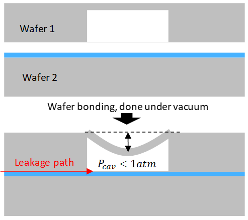
PhilipsMany MEMS devices rely on wafer bonding techniques during their manufacturing e.g., to realize u-fluidic channels, micro-mirrors, and hermetic sealing of inertial sensors that reside in a cavity formed in between the bonded wafers. Wafer bonding techniques typically comprise the formation of a strong interfacial bond between two stacked wafers through fusion, anodic, eutectic, or adhesive bonding. Assessing the bond quality is a challenge since many tests in use today are destructive and/or can only be performed when the device is fully processed.
For more information: flyer
Assignment
This assignment concerns the development of a promising, very sensitive, non-destructive technique to measure the bond quality immediately after the bonding step is performed. The method is based on the notion that the bonding step is done under vacuum and therefore a micro-cavity can be formed between the wafers that is at a pressure level lower than ambient pressure. The method is based on measuring the very small, but detectable, mechanical deflection, or bulging, of the exterior of the micro-cavity caused by this differential pressure.
This assignment addresses the following scientific questions:
- How to use experimental bulge test data to build a physical model of the bond interface?
- How to avoid plastic deformation of the bulging membrane?
- How to use test data to model time-to-failure of the MEMS device?
Tasks:
- To design and test generic mechanical layouts that can be processed on wafer level and be used for in-line bulge testing of wafer bond quality
- To correlate bulge test data with other bond quality measurement techniques, such as Scanning Acoustic Microscopy (SAM) and IR Transmission Microscopy, to build up in-depth knowledge of bond failing mechanisms
- Develop and validate a physical model for the bond interface, based on bulge test and other experimental data
- It is expected that the candidate will be (at least part-time) performing the work at the Philips MEMS foundry location in Eindhoven
Contact
dr.ir. Sten Vollebregt
Electronic Components, Technology and Materials Group
Department of Microelectronics
Last modified: 2023-12-05